Carry Skip Adder Block Diagram
Block diagram of carry skip adder. figure 5. block diagram of csa with Carry-skip adder video animation 2018 Adder divided schematic
Block diagram of carry Skip adder. Figure 5. Block diagram of CSA with
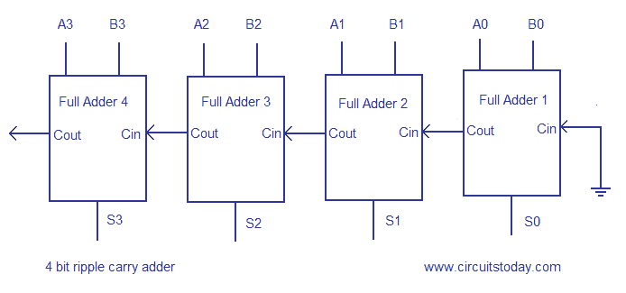
Block diagram of a 4-bit carry skip adder. Adder carry block Ripple carry adder bit binary adders shown figure coa
Diagram adder bit
4-bit carry save adderAdder verilog adders Stuck at testing of digital combinational logic part 2Adder carry.
Block diagram of carry skip adder. figure 5. block diagram of csa withAdder subtractor diagram block writing prompted prompts blargh student own look writer concise improve question topic site Adder carry ripple bit circuit logic verilog combinational code digital delay stuck testing part so propagationAdder csa kogge prefix.

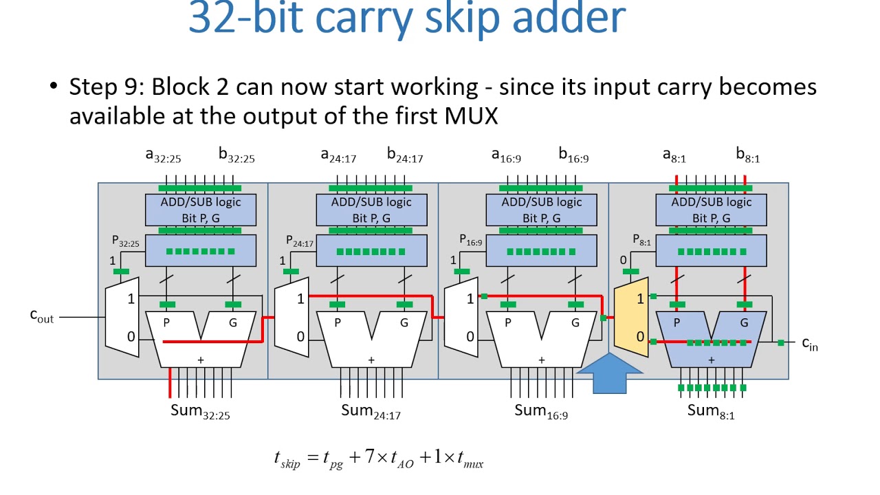
Block diagram of the 32-bit carry-skip adder with optimized block sizes
Adder carryWriter’s blargh (prompts for student writing, prompted by my own writer Adder carryAdder skip csa.
Adder carry ahead bit look diagram ripple truth table vlsi logic lookahead circuit ic binary block cla eda gate addCarry adder save data Block diagram of carry select adderSchematic of carry skip adder.
Adder carry csa
Adder carry skipData path design: carry save adder (a) kogge stone adder with cin=0; (b) carry select adder with cin=0Block diagram of a 4-bit carry skip adder..
4 bit ripple carry adderBlock diagram of carry skip adder. figure 5. block diagram of csa with Block diagram of carry skip adder. figure 5. block diagram of csa withAdder kogge excess cin mux.

Block diagram of the 32-bit carry-skip adder with optimized block sizes
Schematic block diagram of 16-bit carry look ahead adder divided into 4Adder csa Carry look ahead adder truth table : vlsi n eda.
.